Reverse Voltage Protection for Battery Chargers

12V 24V 36V Automatic Baterry Charger Short Circuit Protection Reverse Battery Protection
| Topics covered in this article: |
| Ⅰ. Introduction |
| Ⅱ. N-Channel MOSFET Design |
| Ⅲ. P-Channel MOSFET Design |
| Ⅳ. Summary |
Ⅰ. Introduction
There are a few well-known approaches to dealing with supply voltage inversion. The most obvious solution is to connect a diode between the power source and the load, but the diode's forward voltage will result in increased power dissipation. Diodes are unsuccessful in portable or backup applications since the battery must sink current when charging and supply current when not charging, despite the fact that this method is elegant.
Another way is to use one of the MOSFET circuits shown in Figure 1.

Figure. 1 Traditional Load-Side Reverse Protection
This technique is superior to utilizing diodes for load-side circuits because the supply (battery) voltage boosts the MOSFET, resulting in reduced voltage drop and significantly higher conductance. Because discrete NMOS transistors have stronger conductivity, cheaper cost, and better availability, the NMOS version of this circuit outperforms the PMOS version. When the battery voltage is positive, the MOSFET in both circuits turns on, and when the battery voltage reverses, it disconnects. Because the PMOS variant has a higher potential and the NMOS version has a lower potential, the physical "drain" of the MOSFET becomes the power supply. MOSFET s conduct current well in both directions because they are electrically symmetrical in the triode region. The transistor must have a maximum VGS and VDS rating above the battery voltage when utilizing this method.
Unfortunately, this solution only works with load-side circuits and does not function with battery-charging circuits. The battery charger will provide power, re-enable the MOSFET. and restore the reverse battery connection. Figure 2 illustrates an example of the NMOS version in action, with the battery in a failed state.

Figure. 2 Load-side Protection Circuit with One Battery Charger
The battery charger is turned off when the battery is plugged in, and the load and battery charger are safely detached from the reverse battery. When the charger is turned on (for example, with an input power connector attached), a voltage is created between the gate and source of the NMOS, which improves the NMOS' ability to conduct current. Figure 3 depicts this in further detail.

Figure. 3 Traditional Reverse Battery Protection Schemes are Ineffective for Battery Charger Circuits
Although the load and charger are protected from reverse voltage, the protective MOSFET s suffer from high power dissipation. The battery charger then becomes a battery discharger. When the battery charger provides enough gate support for the MOSFET to sink the charger's current, the circuit will attain equilibrium. The battery charger output voltage will be regulated at 2V (the drain of the MOSFET is at 2V + the battery voltage) if the VTH of a powerful MOSFET is about 2V and the charger can supply current at 2V. ICHARGE•(VTH+VBAT) is the power dissipation in the MOSFET, This causes the MOSFET to heat up and dissipate away from the printed circuit board. The same goes for the PMOS version of this circuit.
Two alternatives to this method are presented below, each with its own advantages and disadvantages.
Ⅱ. N-Channel MOSFET Design
The first solution uses an NMOS isolation device, as shown in Figure 4.
The isolation MOSFET must be disabled if the battery voltage exceeds the battery charger output voltage, according to the circuit's algorithm.
MN1 is connected on the low side of the wire between the charger/load and battery terminals in this circuit, just as it is in the NMOS approach described above. In the event of a reverse battery connection, however, transistors MP1 and Q1 now offer a detecting circuit that disables MN1. By reversing the battery, the source of MP1 rises above its gate, which is connected to the charger's positive terminal. The drain of MP1 then supplies current to the base of Q1 via R1. The gate of MN1 is then shunted to ground by Q1, preventing charging current from flowing in MN1. During reverse detection, R1 is in charge of managing the base current flowing to Q1, while R2 is in charge of providing bleeder for Q1's base during normal operation. Q1 is given permission by R3 to pull MN1's gate to ground potential. The R3/R4 voltage divider controls the voltage on MN1's gate, allowing the gate voltage to drop less during reverse battery hot swap. The worst case scenario is when a reversed battery is connected to a battery charger that is already running and providing its constant voltage level. MN1 must be turned off as soon as feasible in this instance to decrease the amount of time that high power is spent. R3 and R4 in this version of the circuit are best suited for 12V lead-acid battery applications, but R4 can be omitted in lower voltage applications such as single-cell and two-cell Li-Ion devices. During reverse battery attach, capacitor C1 acts as an ultra-fast charge pump, lowering the gate level of MN1. When a reverse battery is connected, C1 is useful in worst-case scenarios where the charger is enabled again.
The disadvantage of this circuit is that it necessitates the use of additional components, and the R3/R4 divider places a minor but consistent strain on the battery.
The majority of such components are small. MP1 and Q1 are not power devices and are often packaged in SOT23-3, SC70-3, or smaller SOT23-3, SC70-3, or smaller SOT23-3, SC70-3, or smaller SOT23-3, SC70-3, or smaller S Because MN1 is a transmission device, it should have excellent conductivity, but it does not need to be particularly large. Even for moderately conductive devices, its power dissipation is low because it operates in the deep triode region and has strong gate reinforcement. Transistors with a width of less than 100m, for example, are frequently packaged in SOT23-3.

Figure. 4 A possible Reverse Battery Circuit
However, utilizing a tiny pass transistor has the disadvantage of increasing the charging time during the constant voltage charging phase due to the increased resistance in series with the battery charger. The charging duration during the constant voltage charging phase will be increased if the battery and its wiring have an equivalent series resistance of 100m and a 100m isolation transistor is employed.
MP1 and Q1's detection and deactivation circuits aren't very quick at deactivating MN1, and they don't have to be. During reverse battery attachment, MN1 consumes a lot of power, yet the shutdown circuit simply disconnects MN1 "at the end." MN1 must be disconnected before it heats up to the point of causing harm. It's possible that a disconnect time of tens of microseconds is sufficient. However, disabling MN1 before the reversed battery has a chance to pull the charger and load voltages negative is crucial, therefore C1 is required. The circuit essentially has one AC and one DC disabled path.
A lead acid battery and the LTC4015 battery charger were used to test this circuit. When the reverse battery is hot-swapped, the battery charger is turned off, as shown in Figure 5. The charger and load are not affected by the reverse voltage.
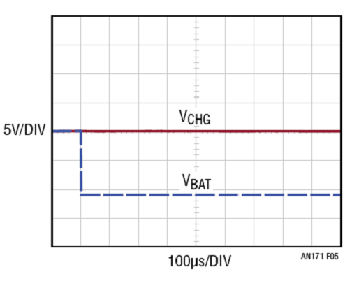
Figure. 5 NMOS Protection Circuit with Charger in off State
It's worth mentioning that MN1 requires a VDS of the same voltage as the battery and a VGS of 1/2 the battery voltage. MP1 requires a VDS and VGS rating of the same voltage as the battery.
When the reverse battery is hot-swapped, Figure 6 depicts a more serious condition in which the battery charger is already in regular operation. A reverse battery connection lowers the charger's voltage until the detecting and protection circuits shut it down, allowing the charger to safely restore to its constant voltage level. The dynamics will differ from one application to the next, and the capacitance of the battery charger will have a significant impact on the final output. The battery charger in this test has a high-Q ceramic capacitor and a lower-Q polymer capacitor.
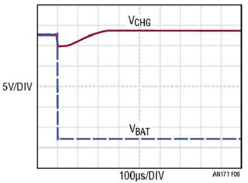
Figure. 6 NMOS Protection Circuit with Charger Running
Finally, on battery chargers, aluminum polymer and aluminum electrolytic capacitors are advised to boost performance during routine positive battery hot swap. Due to their severe nonlinearity, pure ceramic capacitors incur considerable overshoot during hot swapping; the reason for this is that their capacitance declines by an astounding 80% as the voltage goes from 0V to rated voltage. This nonlinearity causes a fatal combination of fast current flow at low voltages and rapid capacitance decrement as the voltage rises, resulting in very high voltage overshoots. The most resilient combination appears to be a ceramic capacitor paired with a lower-Q, voltage-stabilized aluminum capacitor or even a tantalum capacitor.
Ⅲ. P-Channel MOSFET Design
Figure 7 shows the second method, which uses a PMOS transistor as a protection device.
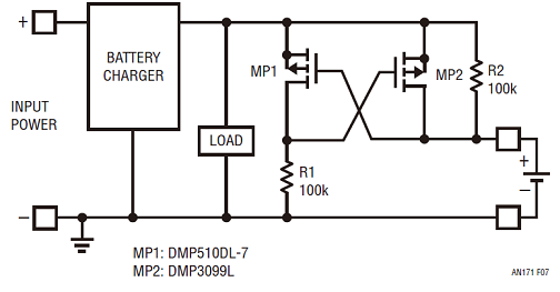
Figure. 7 PMOS Transistor Pass Element Version
MP1 is the reverse battery detection device, while MP2 is the reverse isolation device in this circuit. Compare the positive terminal of the battery to the battery charger output using MP1's source-to-gate voltage. MP1 will disable the main transfer device MP2 if the battery charger terminal voltage is higher than the battery voltage. As a result, if the battery voltage is driven below ground, the detection device MP1 will clearly cause the pass device MP2 to turn off (disturb its gate to its source). Regardless of whether the battery charger is enabled and creating charging voltage or not, this is done (0V).
The most significant benefit of this circuit is that the PMOS isolation transistor MP2 has no authority to supply negative voltages to the charger circuit or load. Figure 8 shows this in greater detail.
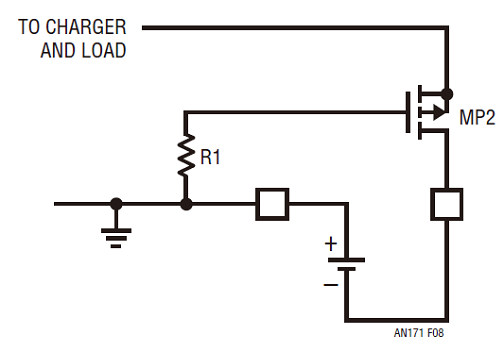
Figure. 8 Illustration of the Cascode Effect
Through R1, the lowest voltage achievable on the gate of MP2 is 0V. Despite the fact that MP2's drain is dragged well below earth, the source does not exert substantial voltage downward pressure. The transistor will de-bias itself and its conductivity will fade away until the source voltage drops to VTH, where the transistor is above ground. The higher the degree of de-biasing of the transistor, the closer the source voltage is to ground. This characteristic, together with the straightforward topology, makes this approach more appealing than the NMOS approach discussed previously. It has the disadvantages of lesser conductivity and higher cost of PMOS transistors when compared to the NMOS approach.
This circuit has one big disadvantage, despite being simpler than the NMOS technique. While it always protects against reverse voltage, the circuit may not always be connected to the battery. The circuit generates a latched storage element when the gates are cross-coupled as indicated, which has the ability to pick the incorrect state. There is a case when the charger produces a voltage (say 12V), the battery is connected at a lower voltage (say 8V), and the circuit is unplugged, which is difficult to perform.
MP1's source-to-gate voltage is +4V in this scenario, which strengthens MP1 while disables MP2. Figure 9 depicts this circumstance, with the node's steady voltage given.
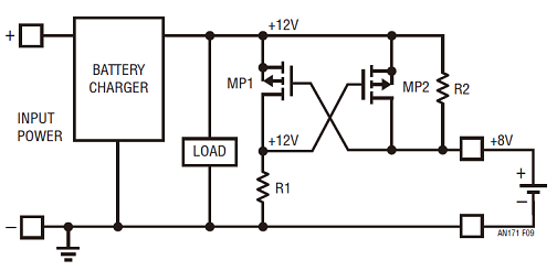
Figure. 9 Diagram of Possible Blocking States When Using a PMOS Protection Circuit
When the battery is attached, the charger must already be running to attain this situation. If the battery is connected before the charger is turned on, the battery pulls up the gate voltage of MP1, thereby deactivating MP1. When the charger is turned on, it creates a controlled current (rather than a large current surge), which decreases the chances of MP1 turning on while MP2 remains off.
If the charger is enabled before the battery is connected, the gate of MP1 simply follows the battery charger output, as the bleeder resistor R2 pulls it up. MP1 has no inclination to turn on and take MP2 out of operation when the battery is not plugged in.
When the charger is already turned on and the battery is connected, the problem occurs. In this instance, there is a brief voltage difference between the charger output and the battery terminals, causing MP1 to disable MP2 when the charger capacitor sinks due to the battery voltage. This results in a struggle between MP2's capacity to suck charge from the charger capacitor and MP1's ability to disable MP2.
A lead acid battery and the LTC4015 battery charger were also used to test the circuit. A "disconnected" condition will never be triggered by connecting a severely loaded 6V source like a battery emulation to an already enabled battery charger. The tests performed are insufficient, and important applications should be extensively tested. Even if the circuit locks, disconnecting and re-enabling the battery charger will always result in a reconnect.
Making a temporary connection between the top of R1 and the output of the battery charger can be used to indicate the fault situation. This circuit, on the other hand, is thought to be more prone to connections. If a connection failure occurs, a circuit can be created that disables the battery charger using several devices. A more full circuit is shown in Figure 12.
With the charger turned off, Figure 10 demonstrates the effect of the PMOS protection circuit.
It's important to note that the battery charger and load voltage will never encounter negative voltage transfer.
In the adverse circumstance of "charger already running when reverse battery is hot-swapped," Figure 11 depicts the circuit
The reverse battery, like an NMOS circuit, draws down the charger and load voltages somewhat before disconnecting the circuit and turning off the pass transistor MP2.
Transistor MP2 must be able to tolerate VDS twice the battery voltage (one for the charger and one for the reverse battery) and VGS equal to the battery voltage in this version of the circuit. MP1 must, on the other hand, sustain a VDS equal to the battery voltage and a VGS double the battery voltage. This is bad because the rated VDS of MOSFET transistors always surpasses the rated VGS. For lead-acid battery applications, transistors with 30V VGS and 40V VDS tolerances are available. To support higher voltage batteries, the circuit must be modified by adding a Zener diode and a current-limiting resistor.
Figure 12 shows an example of a circuit capable of handling two lead-acid batteries stacked in series.

Figure. 10 PMOS Protection Circuit with Charger off
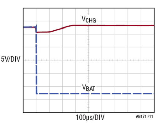
Figure. 11 PMOS Protection Circuit with Charger Running
Analog Devices is confident in the accuracy and reliability of the data it offers. Analog Devices, on the other hand, is not liable for its use or any violation of third-party patents or other rights that may occur as a result of it. Specifications may change at any time without notice. By implication or otherwise, no license to ADI is granted under any patents or patent rights.
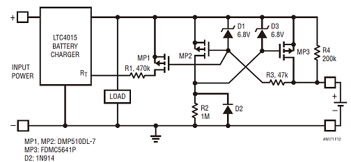
Figure. 12 Higher Voltage Reverse Battery Protection
The gates of MP2 and MP3 are protected against high voltage damage by D1, D3, and R3. When a reversed battery is hot-swapped, D2 prevents the MP3's gate and the battery charger's output from fast dropping below the earth. When the circuit has a reversed battery or is in a false disconnect lockout, MP1 and R1 use the LTC4015's missing RT function to disable the battery charger.
Ⅳ. Summary
For battery charger-based applications, a reverse voltage protection circuit can be designed. Some circuits were created and tested briefly, and the findings were promising. Although there is no magic answer to the reverse battery problem, maybe the approach provided in this post provides enough knowledge that a simple, low-cost solution exists.
1. What are the types of battery chargers?
There are many types of battery chargers: rechargeable alkaline battery chargers, nickel-metal hydride battery chargers, and nickel-cadmium battery chargers.
2. Is the battery charger universal?
Different brands of NiMH battery chargers are completely compatible with each other. However, it is necessary to carefully look at the output current of the charger and the capacity of the battery, and calculate the charging time according to the following method: Calculation of charging time: first look at the output current of the charger and the capacity of the battery, and then divide the capacity of the battery by the capacity of the charger The output current is measured in hours, and a little bit more when actually charging.
3. What does the blinking battery charger mean?
The charging mode of each charger is different, there is a flashing red light when full, and a green light when full.
There are many styles of charger indicator display:
1. The red light is always on when the charger is charging, and it turns green when it is fully charged;
2. The red light flashes when the charger is charging, and the green light turns on when fully charged;
3. The red and green lights flash alternately when the charger is charging, and both red and green lights are on when fully charged.
4. When the charger is charging, two red lights are always on, and one red light and one green light are on when fully charged.
 Discovering New and Advanced Methodology for Determining the Dynamic Characterization of Wide Bandgap DevicesSaumitra Jagdale15 March 20242179
For a long era, silicon has stood out as the primary material for fabricating electronic devices due to its affordability, moderate efficiency, and performance capabilities. Despite its widespread use, silicon faces several limitations that render it unsuitable for applications involving high power and elevated temperatures. As technological advancements continue and the industry demands enhanced efficiency from devices, these limitations become increasingly vivid. In the quest for electronic devices that are more potent, efficient, and compact, wide bandgap materials are emerging as a dominant player. Their superiority over silicon in crucial aspects such as efficiency, higher junction temperatures, power density, thinner drift regions, and faster switching speeds positions them as the preferred materials for the future of power electronics.
Read More Applications of FPGAs in Artificial Intelligence: A Comprehensive GuideUTMEL29 August 2025514
This comprehensive guide explores FPGAs as powerful AI accelerators that offer distinct advantages over traditional GPUs and CPUs. FPGAs provide reconfigurable hardware that can be customized for specific AI workloads, delivering superior energy efficiency, ultra-low latency, and deterministic performance—particularly valuable for edge AI applications. While GPUs excel at parallel processing for training, FPGAs shine in inference tasks through their adaptability and power optimization. The document covers practical implementation challenges, including development complexity and resource constraints, while highlighting solutions like High-Level Synthesis tools and vendor-specific AI development suites from Intel and AMD/Xilinx. Real-world applications span telecommunications, healthcare, autonomous vehicles, and financial services, demonstrating FPGAs' versatility in mission-critical systems requiring real-time processing and minimal power consumption.
Read More Advanced CMOS Devices with Wide Bandgap and Ultrawide Bandgap TechnologiesSaumitra Jagdale15 March 20242883
Power and radio frequency electronics play an increasingly important role in energy-efficient and collaborative future as there is always a demand for faster, smaller, high-voltage and more conductive transistors. Traditionally, silicon has been the semiconductor of choice due to its extensive research and manufacturing history, and natural abundance. While silicon power devices continue to maximize performance, many applications are now integrating wider-band gap semiconductors. These materials offer a significantly higher voltage-conducting capacity, surpassing silicon's limits in tradeoffs related to ON-resistance, capacitances, and breakdown voltage.
Read More FPGA in Industry and Communication: Key Players, Technologies, and Future TrendsUTMEL07 March 20251051
FPGAs (Field Programmable Gate Arrays) have become the core hardware in the industrial and communication fields due to their programmability and parallel processing capabilities.
Read More Designing Application-Specific Integrated CircuitsRakesh Kumar, Ph.D.07 March 20251331
This article explores the design process, benefits, and roles of Application-Specific Integrated Circuits in enhancing performance and efficiency in embedded systems.
Read More
Subscribe to Utmel !
![ISD203XG]() ISD203XG
ISD203XGIsocom Components
![IS829SM]() IS829SM
IS829SMIsocom Components
![ILQ5XSMT&R]() ILQ5XSMT&R
ILQ5XSMT&RIsocom Components
![ISP847XASM]() ISP847XASM
ISP847XASMIsocom Components
![PS2502-4XSM]() PS2502-4XSM
PS2502-4XSMIsocom Components
![PS2502-2XSM]() PS2502-2XSM
PS2502-2XSMIsocom Components
![TIL196AX]() TIL196AX
TIL196AXIsocom Components
![TIL116XG]() TIL116XG
TIL116XGIsocom Components
![TIL114XSMT&R]() TIL114XSMT&R
TIL114XSMT&RIsocom Components
![TLP621-2GRSM]() TLP621-2GRSM
TLP621-2GRSMIsocom Components


